PCBAs supplied by S & Q Europe B.V. are conforming to the latest version of following standards, and of standards referenced therein.
| IPC-6010 | Series of Performance Specification for PCBs. |
| IPC-A-600 | Acceptability of Printed Boards. |
| IPC-A-610 | Acceptability of Electronic Assemblies. |
| IPC-J-STD-003 | Solderability tests for printed boards. |
| IPC/JEDEC-J-STD-609 | Marking and labelling of components, PCBs and PCBAs to Identify Lead (Pb), Pb-free and Other Attributes. |
| IPC-9252 Level B | Electrical test for bare boards. |
Disclaimer:
All information is provided on an as is basis. Although supplier has done it utmost to have this information complete and correct, supplier cannot be held responsible for any incorrect and/or incomplete information. Supplier can never be held responsible for any damages resulting from the use of this information. Supplier has the right to alter this information at any time without notice.
2.1.
The assembly shop is dedicated to do a fast turnaround of assembly projects with focus on Quality and Flexibility.
2.2.
PCBA are conform IPC610, Class II, ISO9001
2.3.
All bare PCBs are conforming to EC-Regulation nr. 1907/2006 – REACH.
No substances classified as “Substances of Very High Concern” (SVHC) present.
All components are conforming to EC-Regulation nr. 1907/2006 – REACH
2.4.
All bare PCBs are conforming to Directive 2011/65/EU of the European Parliament and of the Council, RoHS 2 (Restriction of Hazardous Substances).
All components are, unless specific components are specified, conforming to Directive 2011/65/EU of the European Parliament and of the Council, RoHS 2
2.5.
Unless explicitly specified otherwise:
| PCB | Printed circuit board not populated |
| PCBA | Printed circuit board populated with components |
| PCS | Single piece printed circuit board |
| Panel | Composition of one or more pieces (PCS) PCB of the same design |
| Tooling | A set of data / films / masks to manufacture the PCB |
| Stencil | To apply the solder paste on the PCB |
| NRE | Non-recurring engineering cost (all one-time cost made to execute the project, stencil and tooling can be part of it) |
| CoC | Certificate of Conformity |
| BGA | Ball Grid Array |
| SOT | Small-Outline Transistor |
For all documents the latest version with the latest date is valid for production.
NOTE: In case of a conflict the customer will be contacted before starting production.
| Positioning | Soldering | ||||
|---|---|---|---|---|---|
| Manual | By means of Equipment* | Manual | Vapour Phase | Vacuum Vapour Phase | |
| BGA >0,4mm pitch | |||||
| BGA ≤ 0,4mm pitch | |||||
| ICs ≥ 0,3mm pitch | |||||
| ICs < 0,3mm pitch | |||||
| SMD ≥ shape 01005 | |||||
| Press-fit components | |||||
| Wire bonding | |||||
| Cleaning of PCBA | |||||
| Assembly Rigid PCB | |||||
| Assembly Rigid Flex | |||||
| Assembly Rigid Flex-Rigid | |||||
| Assembly Stretch (Stretch-rigid) | |||||
| Thickness PCB <=3,6 mm | |||||
| Thickness PCB >3,6 mm | |||||
| Specific packages | |||||
| SOT1232 | |||||
| in mm | with | depth | hight |
|---|---|---|---|
| UV Laser | 660 | 600 | |
| CNC drill/rout | 400 | 620 | |
| Line Iineo | 700 | 460 | |
| Line Finesse | 500 | 400 | |
| Vapour phase vacuum 230°C | 650 | 650 | |
| Netto screen | 600 | 650 | |
| Selective soldering 295°C | 600 | 500 | |
| 180 degrees turned | 700 | 500 | |
| Fluxshooter | 600 | 600 | |
| Washing | 530 | 530 | 520 |
| Washing max | 700 | 500 | |
| Stove | 1000 | 500 | 1200 |
| Vacuum stove | 500 | 400 | |
| AOI Saki 3D | 500 | 450 | |
| Measuring table | 700 | 600 | |
| SEM | 100 | 100 | 50 |
| Rontgen rotating | 500 | 400 | |
| Rontgen flat | 640 | 500 | |
| Kelvin probe testing | 700 | 600 | |
| Bonding station for Repair station BGA/LGA | 300 | 200 |
The Service Centre is specially organized to cope with very different projects. Therefore, for all projects a project leader is appointed. The project leader takes care of:
| 7.1. | Visual inspection system |
| 7.2. | 3D X-Ray inspection |
| 7.3. | No functional test |
| 7.4. | Interconnection test optional |
| 8.1. | ESD safe work spaces + ESD test equipment |
| 8.2. | Manual soldering stations |
| 8.3. | Stereo Microscopes |
| 8.4. | Pasta dispensing / screener, maximum dimensions TBD |
| 8.5. | Pre-heater |
| 8.6. | Wire bond machine (manual/automatic) |
| 8.7. | Iineo plus pick & placer |
| 8.8. | Vapour phase soldering from Rehm and Ascon, maximum dimensions: 650 x 650mm |
| 8.9. | Fluxshooter from Interflux |
| 8.10. | Selective soldering from Ersa |
| 8.11. | PCBA Cleaning machine |
| 8.12. | Cleanroom and many flow cabinets with 0 particles >= 0.05 um |
Lead free and suitable for lead free soldering materials and components are used unless specified otherwise.
| 11.1. | The PCBs are electrically tested, according IPC-9252 Level B. |
| 11.2. | Components from A class distributors are used. |
| 11.3. | All PCBAs are visually inspected for correct components, correct placing of components and quality of the soldering joints. |
| 11.4. | As the product is not functionally tested, complaints on malfunction of the PCB are not accepted which are outside the scope of activities of S & Q Europe Model-shop. |
Phone: +31(0)492 598484
General: info@sq-europe.com
Buying: purchase@sq-europe.com
Sales: sales@sq-europe.com
Quality: quality@sq-europe.com
Finance :finance@sq-europe.com
Jeroen Charmant: Jeroen.Charmant@sq-europe.com
John Geenen: John.geenen@sq-europe.com
Maurice Keulers: Maurice.Keulers@sq-europe.com
| Production standards (tolerances) | According to standards: IPC-A-600 Class 2 (The standard is available on request) |
| Number of PCB layers | 1-12 layers Layer build-up according to requirements - Selection |
| Minimum track and gap size | Minimum track width / isolation gap: 0.1 mm |
| Drilling | Minimum drill diameter: 0.2 mm (PTH 0.15 mm) Aspect ratio: 1:12 |
| Soldermask | Colors: green, blue, red, white, black |
| Silk screen | Colors: green, blue, red, white, black |
| Surface treatment | lead-free HAL HAL SnPb chemical NiAu |
| Mechanical finish | milling V-cut |
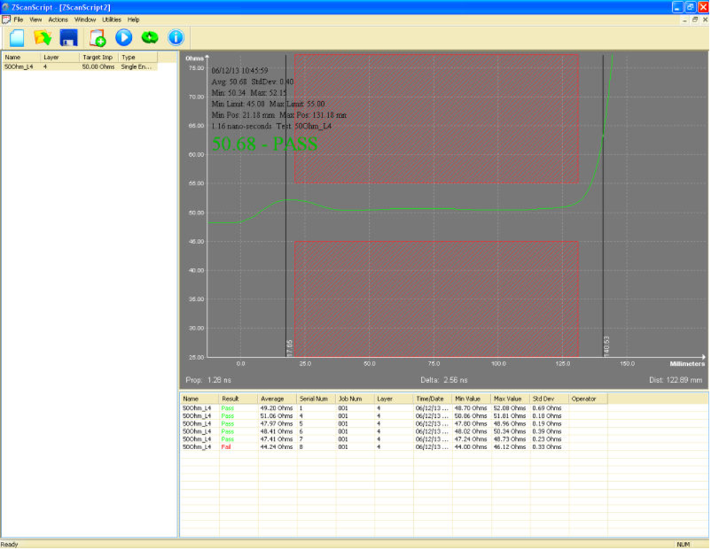
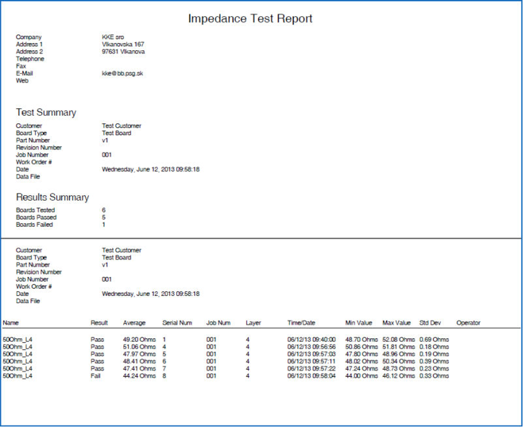
| Testing methods | electrical test optical test- AOI controlled impedance micro sections |
| Further options | Manufacturing Standard IPC-A-600 Class3 UL certification UL-file number:E258735 Controlled impedance according IPC-2141A Total PCB thickness up to 6 mm Edge plating plated half-hole carbon layer removable paint Via-hole filler Z-axis milling Interrupted grooving press-fit holes buried holes blind holes - aspect Ratio 1:1 flexible printed circuit boards - material on stock teflon, ceramic - materials on request |
– RF, Microwave, High Speed Digital PCBs
RF and microwave PCBs are typically built using advanced composites with specific characteristics for dielectric constant Dk, loss tangent Df, and coefficient of thermal expansion (CTE).
High frequency circuit materials with a low stable Dk and loss tangent Df allow for high speed signals to travel through the PCB with less impedance than standard FR-4 PCB materials. These materials can be mixed in the same stack-up for optimal performance and economics.
Our supplier choice for a RF and Microwave PCBs material is isola – a global material sciences company focused on designing, developing, manufacturing and marketing copper-clad laminates and dielectric prepregs used to fabricate advanced multilayer printed circuit boards. Isola high-performance materials are used in a diverse range of electronic end-markets including applications in computers, networking and communications equipment, high-end consumer electronics, as well as products designed for use in the advanced automotive, aerospace, military and medical markets.
The company invests in research and development to create industry-leading products formulated to meet the most demanding performance requirements of its customers, the printed circuit board fabricators, and the designers and original equipment manufacturers (OEMs) they serve. The global footprint includes manufacturing facilities and research centers located in Europe and the United States.
| Isola Product | Dk @ 10GHz | Df @ 10GHz |
|---|---|---|
| I-Tera® MT40 RF | 3.38 | 0.0028 |
| I-Tera® MT40 MW | 3.45 | 0.0030 |
| Competitive material | Dk @ 10GHz | Df @ 10GHz |
|---|---|---|
| Rogers RO4003 | 3.38 | 0.0027 |
| Taconic TLC-338 | 3.38 | 0.0034 |
| Rogers (Arlon 25N) | 3.38 | 0.0025 |
| Nelco NH9338 | 3.38 | 0.0025 |
| Nelco N9530-13RF | 3.38 | 0.0046 |
| Rogers RO4534 | 3.40 | 0.0027 |
| Nelco Meteorwave 1000 | 3.40 | 0.0040 |
| Rogers RO4350B | 3.48 | 0.0037 |
| Rogers RO4350BTX | 3.48 | 0.0034 |
| Rogers RO4835 | 3.48 | 0.0037 |
| Nelco NH9348 | 3.48 | 0.0037 |
| Nelco NH9350-13RF | 3.48 | 0.0055 |
| Thickness [mm] | Dk (2-20 GHz) | Df (2-20 GHz) | Tg (℃) | CTE in Z-Axis (ppm/℃) | Cu type VLP-2 | Cu thick. (μm) | Panel size [mm] |
| Laminate | 0.127 | 3.38 | 0.0028 | 200 | 290 | Rz=2 μm | 18/18 | 275x505 |
| Laminate | 0.254 | 3.38 | 0.0028 | 200 | 290 | Rz=2 μm | 18/18 | 275x505 |
| Laminate | 0.508 | 3.38 | 0.0028 | 200 | 290 | Rz=2 μm | 18/18 | 275x505 |
| Laminate | 0.762 | 3.38 | 0.0028 | 200 | 290 | Rz=2 μm | 18/18 | 275x505 |
| Laminate | 1.016 | 3.38 | 0.0028 | 200 | 290 | Rz=2 μm | 18/18 | 275x505 |
| Laminate | 1.524 | 3.38 | 0.0028 | 200 | 290 | Rz=2 μm | 18/18 | 275x505 |
| Laminate | 0.254 | 3.45 | 0.0030 | 200 | 290 | Rz=2 μm | 18/18 | 275x505 |
| Laminate | 0.508 | 3.45 | 0.0030 | 200 | 290 | Rz=2 μm | 18/18 | 275x505 |
| PR2116 | 0.138 | 3.48 | 0.0031 | 200 | 290 | 59% resin content | 275x505 |
| PR1080 | 0.101 | 3.14 | 0.0022 | 200 | 290 | 73% resin content | 275x505 |
| PR1035 | 0.064 | 3.14 | 0.0022 | 200 | 290 | 73% resin content | 275x505 |
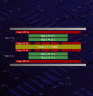
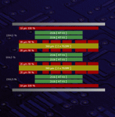
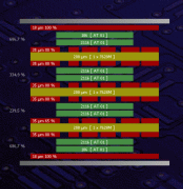
A “Pure build” refers to a multilayer PCB material construction that is composed of the same type of material throughout the stackup.
A „Hybrid build“ could use a mix of Isola PCL370HR high performance material 180°Tg with high-frequency material Isola I-Tera MT40.
The reasons for using a hybrid construction in RF multilayer PCB designs are typically driven by cost, reliability, or electrical performance.
When designs feature a number of noncritical circuit layers, these can usually be built on the more cost-friendly PCL370HR material only using high-frequency RF materials on the critical circuit layers.
Hybrid construction is becoming more popular as technology evolves, but hybrids bring both benefits and challenges that need to be understood. Working closely with the PCB fabricator will ensure the best construction methodology that balances RF performance and PCB manufacturability.
The “fifth generation” of telecommunication systems, or 5G, will be one of the most critical building blocks of our digital economy and society in the next decade. SQP International has taken significant steps to participate in global developments towards this strategic technology.
High speed digital printed circuit boards are key components for devices processing or transmitting high data rates. Typical applications are IC test systems, 5G base stations, internet switches, IoT devices and high speed computing. These systems operate in many cases with data rates of 10Gbit/s or more.

Please select suitable material based on its specs and features – detailed material specification.
| Double sided PCB | Multilayer PCB |
|---|---|
| 325 mm x 582 mm | 274 mm x 505 mm |
| Thickness (laminate thickness) |
Isola DE104 | Isola PCL370HR | |||||
|---|---|---|---|---|---|---|---|
| [mm] | Cu 18/18 | Cu 35/35 | Cu 70/70 | Cu 18/18 | Cu 35/35 | Cu 70/70 | Cu 105/105 |
| 0.075 | |||||||
| 0.100 | |||||||
| 0.125 | |||||||
| 0.150 | |||||||
| 0.200 | |||||||
| 0.300 | |||||||
| 0.360 | |||||||
| 0.410 | |||||||
| 0.460 | |||||||
| 0.560 | |||||||
| 0.610 | |||||||
| 0.710 | |||||||
| 0.900 | |||||||
| 1.000 | |||||||
| Thickness (overall thickness) |
Isola DE104 | Isola PCL370HR | |||||||
|---|---|---|---|---|---|---|---|---|---|
| [mm] | Cu 0/35 | Cu 18/18 | Cu 35/35 | Cu 50/50 | Cu 70/70 | Cu 18/18 | Cu 35/35 | Cu 50/50 | Cu 70/70 |
| 1.00 | |||||||||
| 1.20 | |||||||||
| 1.50 | |||||||||
| 2.00 | |||||||||
| 2.40 | |||||||||
| 3.20 | |||||||||
| Isola DE104 | Isola PCL370HR | |
|---|---|---|
| Type | Pressed thickness [mm] | |
| 106 | 0.057 | 0.045 |
| 1080 | - | 0.065 |
| 2116 | 0.105 | 0.090 |
| 7628 | 0.197 | 0.172 |
| PL05 2116 | - | 0.110 |
| PL04 7628 | - | 0.198 |
| PL05 1080 | - | 0.070 |
| Thickness [um] | Copper Foil |
|---|---|
| 5 | |
| 6 | |
| 12 | |
| 18 | |
| 35 | |
| 50 | |
| 70 | |
| 105 | |
| 140 |
| 106 | 48 µm | 46 µm | 48 µm |
| 1080 | 69 µm | ||
| 2116 | 109 µm | 97 µm | 99 µm |
| 106 | 48 µm | 46 µm | 48 µm |
| Copper foil | |||
|---|---|---|---|
| Thickness [µm] | 312 x 380 mm | 312 x 512 mm | 312 x 600 mm |
| 5 | |||
| 9 | |||
| 12 | |||
| 18 | |||
| 35 | |||
| 50 | |||
| 70 | |||
| 105 | |||
| 140 | |||
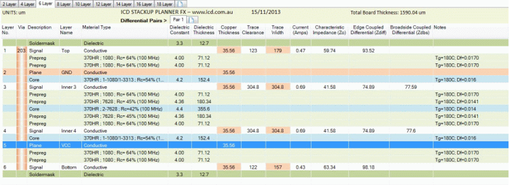
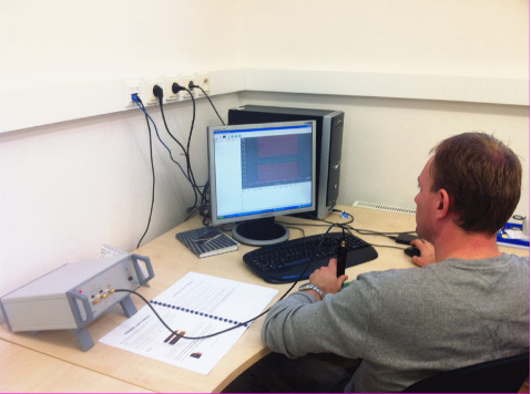
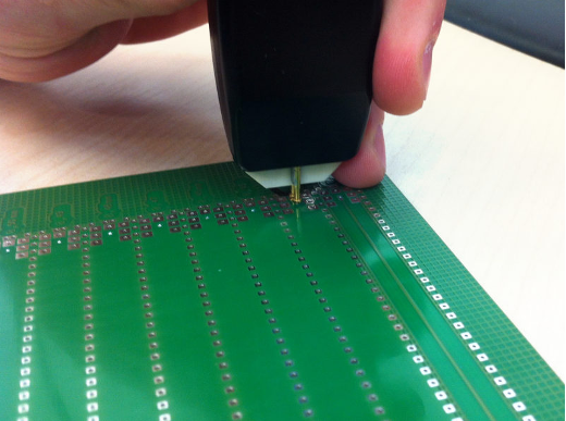
Software for impedance calculation and test coupon design:
ICD Stackup Planner from In-Circuit Design Pty Ltd. (www.icd.com.au)
Controlled impedance measuring device:
Zmetrix ST300 from ZMetrix, Inc. (www.zmetrix.com)
Measurement according IPC-2141A (www.ipc.org)

Tg – Glass Transition Temperature
Temperature point at which a glassy solid changes to an amorfous resin / epoxy
– if temperature exceeds Tg:
1. expansion of the material is growing rapidly in the direction of Z axis
2. mechanical material properties degrade rapidly (strength, bonds in the material)
Td – Decomposition Temperature
Temperature at which there is a 5% weight loss of resin / epoxy
– if temperature exceeds Td:
1. irreversible destruction in material occurs due to breach of chemical bonds in resin / epoxy
T260/T288
Measures time to delamination at specific temperature (i.e. 260°C/288°C)
CTE – Coefficient of Thermal Expansion
Dimensional increasing of the material in the X-, Y-and Z-axis by change of temperature at a constant pressure
CAF – Conductive Anodic Filament
Migration of copper ions through an enclosed moisture in the material, which can over time cause a short circuit
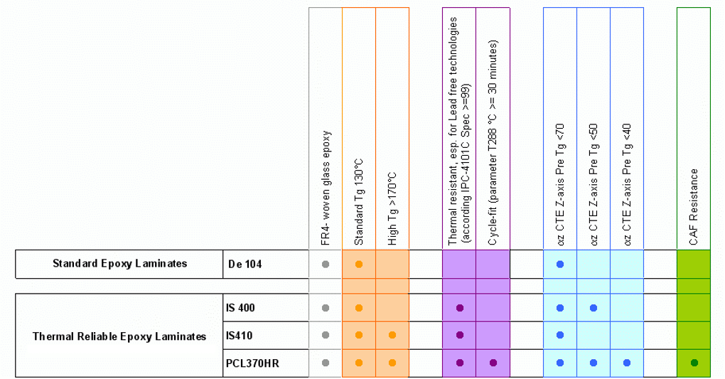
| Isola DE 104 | Isola IS410 | Isola 370HR | |
|---|---|---|---|
| IPC-4101C Spec | 21 | 21/24/26/28/121/124 | 21/24/26/98/99/101/126 |
| Tg Glass Transition Temperature by DSC, spec minimum [°C] | 130 | 175 | 175 |
| Td Decomposition Temperature @ 5% wt loss [°C] | 330 | 350 | 340 |
| T260 Mins | 60 | 50 | 60 |
| T288 Mins | >5 | >10 | 30 |
| CTE, Z-axis Pre Tg | 50 | 65 | 45 |
| % Z-Axis Expansion (50-260C) | 3 | 3.5 | 2.8 |
| CTE, Z-axis Post Tg | 250 | 250 | 230 |
| CTE, Pre X, Y | 13 | 13/14 | 13/14 |
| CTE, Post Tg X, Y | 14 | 15/17 | 14/17 |
| Thermal Conductivity | 0.4 | 0.5 | 0.4 |
| Thermal Stress 10 Sec @ 288°C (550.4°F), spec min | pass | pass | pass |
| Permittivity (Dk) 100 MHz HP4285A | 4 | 3.96 | 4.24 |
| Permittivity (Dk) 1 GHz HP4291A | 4 | 3.9 | 4.17 |
| Permittivity (Dk) 2 GHz Bereskin Stripline | 4 | 3.97 | 4.04 |
| Permittivity (Dk) 5 GHz Bereskin Stripline | 4 | 3.87 | 3.92 |
| Permittivity (Dk) 10 GHz Bereskin Stripline | 3.59 | 3.87 | 3.92 |
| Loss Tangent (Df) 100 MHz HP4285A | 0.02 | 0.0149 | 0.015 |
| Loss Tangent (Df) 1 GHz HP4291A | 0.02 | 0.0189 | 0.0161 |
| Loss Tangent (Df) 2 GHz Bereskin Stripline | 0.022 | 0.02 | 0.021 |
| Loss Tangent (Df) 5 GHz Bereskin Stripline | 0.02 | 0.023 | 0.025 |
| Loss Tangent (Df) 10 GHz Bereskin Stripline | 0.02 | 0.023 | 0.025 |
| Volume Resistivity (After moisture resistance) | 1.3x10^8 | 5.0x10^8 | 3.0x10^10 |
| Volume Resistivity (At elevated temperature) | 3.4 x10^3 | 3.6 x10^5 | 7.0 x10^8 |
| Surface Resistivity (After moisture resistance) | 1.0x10^8 | 8.0x10^5 | 3.0x10^8 |
| Surface Resistivity (At elevated temperature) | 7.0x10^8 | 4.5x10^8 | 2.0x10^8 |
| Dielectric Breakdown, spec minimum | >50 | >50 | >50 |
| Arc Resistance, spec minimum | 120 | 129 | 115 |
| Electric Strength, spec minimum (Laminate & prepreg as laminated) | 54 (1350) | 44 (1100) | 54 (1350) |
| Comparative Tracking Index (CTI) | 2 [250 - 399] | 3 [175 - 249] | 3 [175 - 249] |
| Peel Strength Low profile Cu foil, very low profile – all Cu >17um | 6.5(1.14) | 7 (1.23) | 6 (1.05) |
| Peel Strength Standard profile copper - After thermal stress | 7 (1.23) | 7 (1.23) | 9 (1.58) |
| Peel Strength Standard profile copper - At 125°C (257°F) | 6.5(1.14) | 6.5(1.14) | 7 (1.23) |
| Peel Strength Standard profile copper - After process solutions | 7 (1.23) | 7 (1.23) | 9 (1.58) |
| Flexural Strength Lengthwise direction | 89.00 | 79.00 | 90.00 |
| Flexural Strength Crosswise direction | 70.00 | 68.00 | 77.00 |
| Moisture Absorption, spec maximum | 0.3 | 0.2 | 0.15 |
| Flammability (Laminate & prepreg as laminated), spec min | V0 | V0 | V0 |
| HWI | 0 | ||
| Max Operating Temperature (MOT) [°C] | 130 | 130 (150) | 130 (150) |
| DSR | yes | yes | yes |
The parcel with PCBs will be delivered within 48 hours (2 working days) from receipt of order and data.
In “48hour Service” we supply PCB in standard configuration and low volume.
Day 1: Order and Data receipt before 9.30 >>> Day 2: PCB dispatch by courier >>> Day 3: Delivery of PCB
Superexpress
In “Superexpress mode” PCBs will be manufactured in 3 working days.
Day 1: Order and Data receipt before 9.30 >>> Day 3: PCB dispatch by courier >>> Day 4: Delivery of PCB
Express
In “Express mode” PCBs will be manufactured in 4 working days.
Day 1: Order and Data receipt before 9.30 >>> Day 4: PCB dispatch by courier >>> Day 5: Delivery of PCB
Standard
In “Standard mode” PCBs will be manufactured in 5 working days.
Day 1: Order and Data receipt before 12.00 >>> Day 5: PCB dispatch by courier >>> Day 6: Delivery of PCB
PCB delivery
For comfortable and fast delivery of PCBs, we primarily use the DHL delivery service.
In accordance with the DHL delivery conditions the parcel will be delivered on the next working day after dispatch.