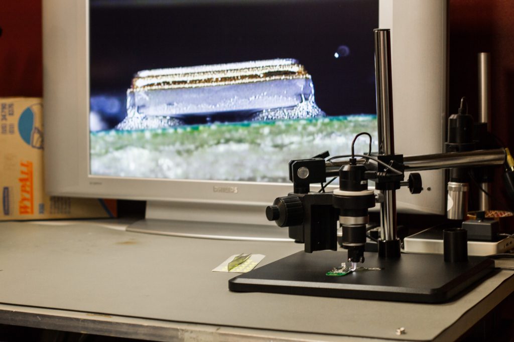
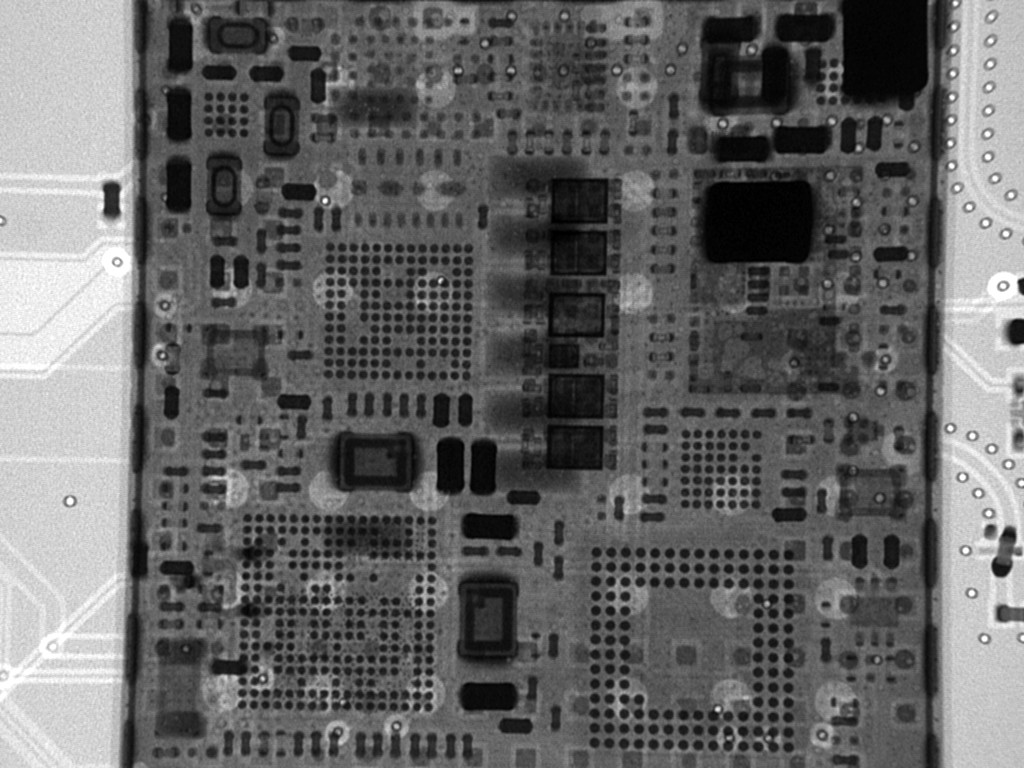
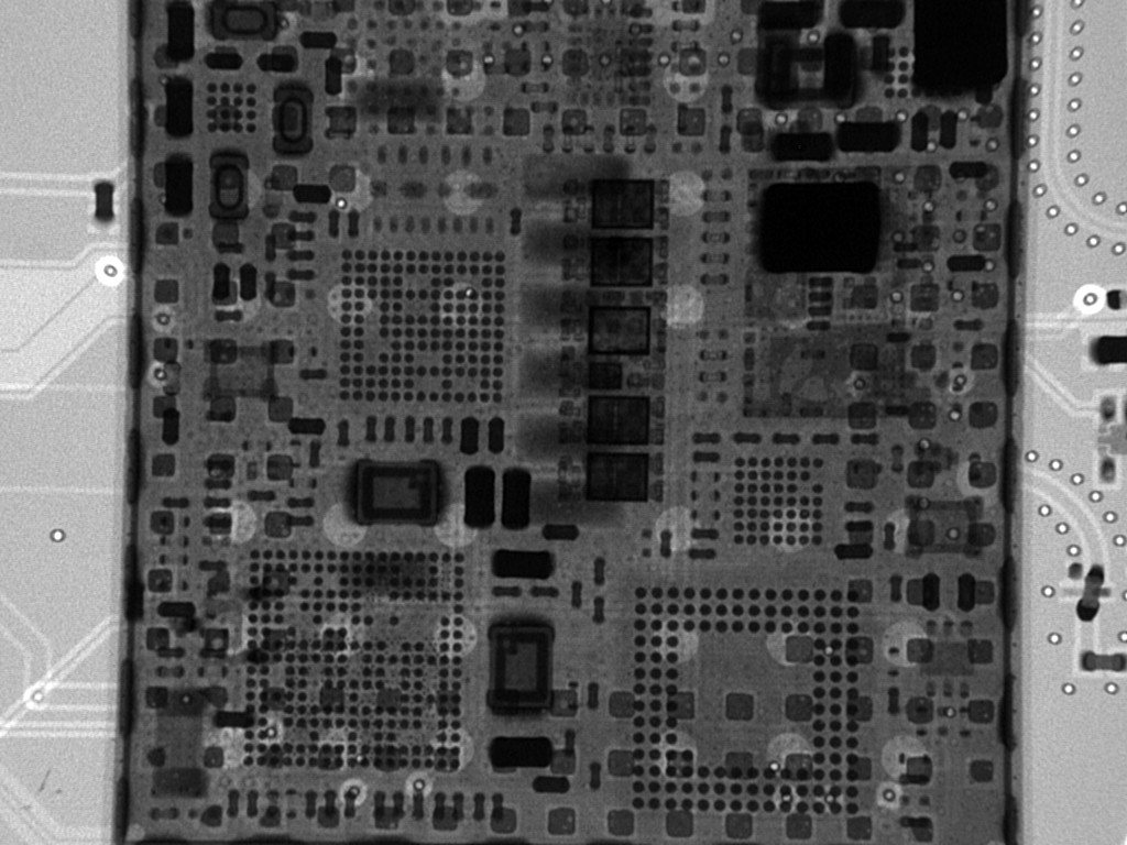
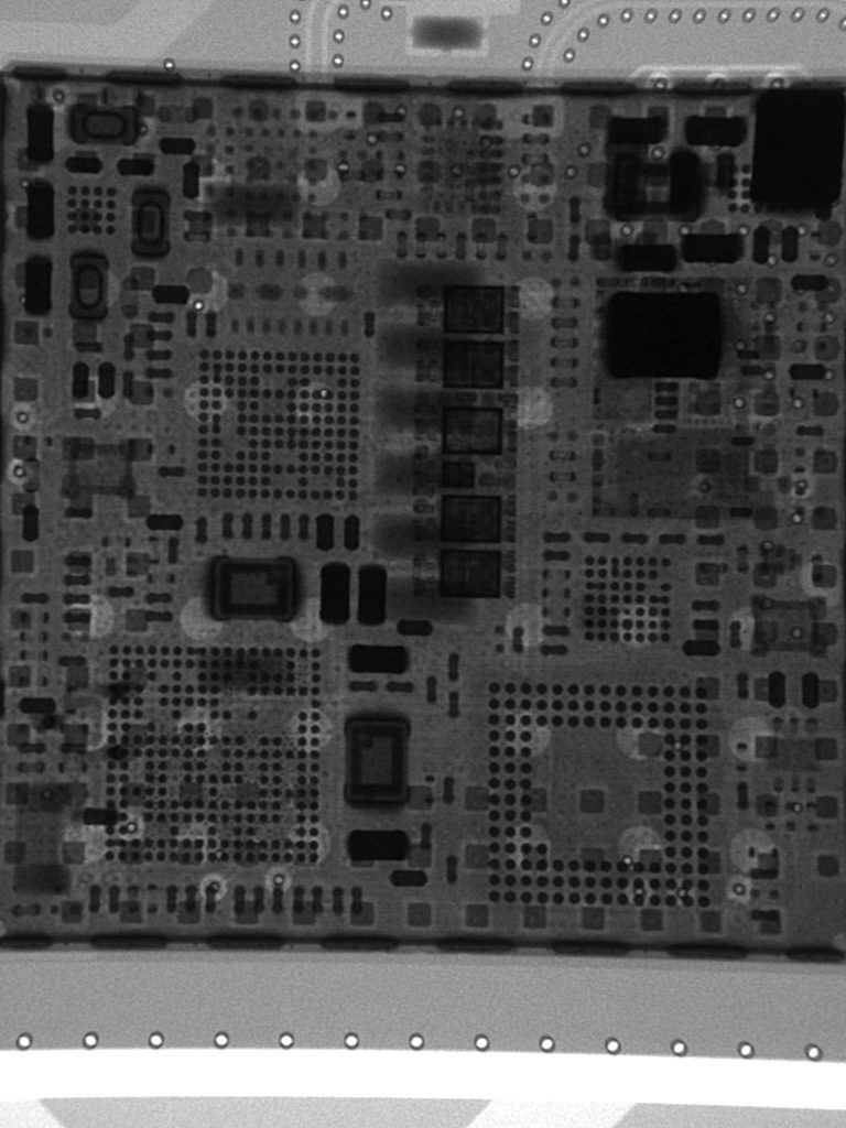
We decided to invest in our own laboratory because we wanted to locate and analyse problems. This service is open to all our customers. It is always good to know and to be able to see what the cause of a problem is. This service uses, among other things, microsection, X-ray to SEM and X-ray microanalysis.
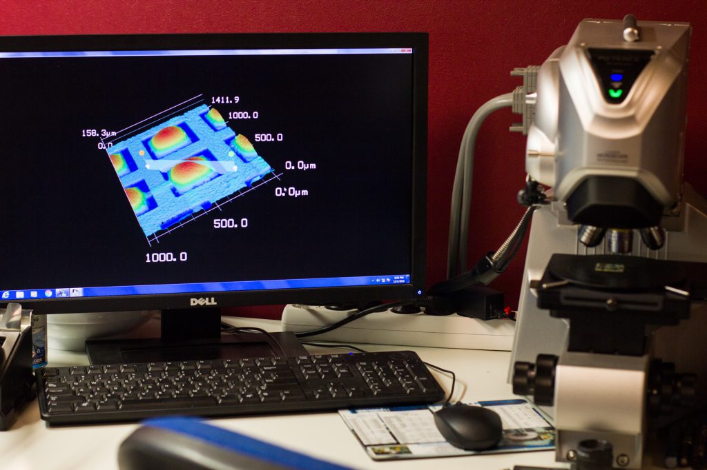
We are able to analyze different kind of alloys. Analysis as big as 100mm x 100mm samples, or more microsections in the same sample holder. On the picture below you can see an example of a microsection in the SEM of a multilayer with a soldered chip.
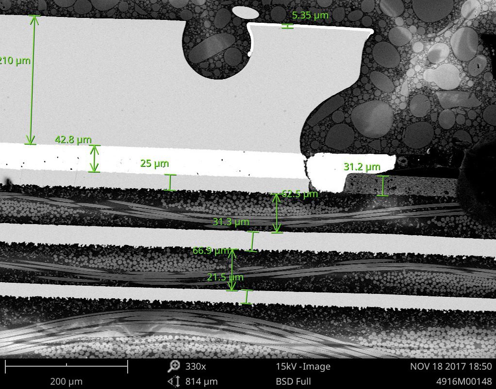
X-ray from LGA repair
From left to right the pictures show an example of a repaired LGA, in the middle with low vacuüm and on the right with high vacuüm. You can clearly see the vacuüm effect on the voids of the LGA pads.
Lorem ipsum dolor sit amet, consectetur adipiscing elit. Ut elit tellus, luctus nec ullamcorper mattis, pulvinar dapibus leo.
Services
In order to be able to deliver “your one stop pcb service centre”, we offer you a wide range of services:
PCB’s, PCBA’s, electrical testing with or without Kelvin, AOI, independant measurements, laboratory, UV laser, CNC drilling/routing, repair or patch work, hand or CNC assembly and chemically washing.